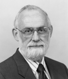
Awardee Interviews | Biography: John F. O'Hanlon
John F. O'Hanlon

John F. O'Hanlon received the AAS from the State University of New York at Farmingdale in 1957, after which he joined IBM Corporation in Poughkeepsie, New York as a laboratory technician. From 1959 to 1963 he was on educational leave at the University of Arizona, where he received the BSEE (1962) and M.S. (1963). He continued his education at Simon Fraser University, where he received the PhD (physics) in 1967, at which time he rejoined IBM's Thomas J. Watson Research Center in Yorktown Heights, NY, as a Research Staff Member.
Dr. O'Hanlon's interest in vacuum technology dates from the late 1950's, when he was a member of the IBM group designing and fabricating large scale lead-tin superconducting circuits. His research interests since then have ranged from fabrication of high speed germanium transistors, plasma anodization of metals and semiconductors, electroluminescent displays, gas panel displays, high resolution multi-beam cathode ray tube fabrication, and vacuum equipment for construction of active matrix liquid crystal displays.
In 1987 he retired from IBM and joined the faculty of Electrical and Computer Engineering at the University of Arizona, where he has been active in research on contamination control relating to semiconductor manufacturing. He is Director of the UA Center for Microcontamination Control, a National Science Foundation Industry-University Cooperative Research Center, where he has built a center with strong industrial ties whose research focuses on wafer cleaning, particle metrology, gas and material contamination, and ultra-pure water metrology. Dr. O'Hanlon was a member of the proposal team for the University of Arizona SEMATECH Center of Excellence in Contamination/Defect Assessment and Control, and is currently a principal investigator of the task on contamination in vacuum processing equipment. His research interests are in the areas of general vacuum equipment contamination, and process specific contamination issues such as ion implanters, plasma deposition and etching systems and the related physics of dusty plasmas.
Professor O'Hanlon is the author or co-author of a number of research papers, and a book. He is a Senior Member of the IEEE, and has seved as Associate Editor of the IEEE Transactions on Semiconductor Manufacturing. Dr. O'Hanlon has served as Chairman of the Vacuum Technology Division (1986), Associate Editor of Journal of Vacuum Science and Technology A, and is an AVS short course instructor. In addition to his research activities, he teaches courses in semiconductor device processing and vacuum systems engineering.